Graphene Oxide Thick Film Reduction by Carbon Dioxide Laser Irradiation on N-type Silicon Wafer
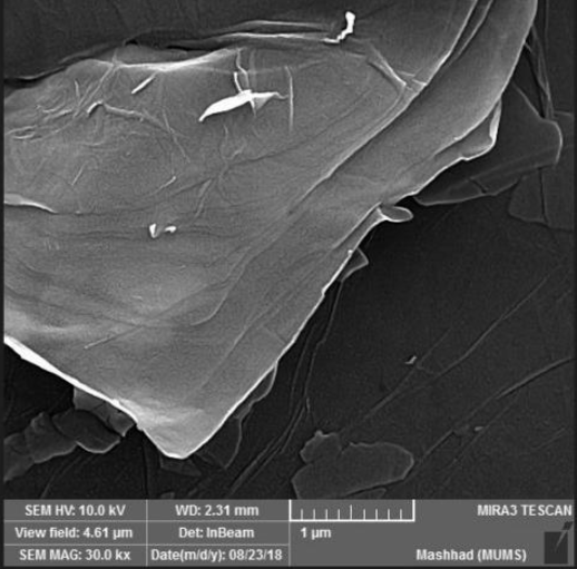
A 50 milliliter colloidal solution of mono layer GO was readily bought from a local market. The concentration of GO was about 5 grams per liter. Following figure demonstrates the FESEM of the colloidal GO solution, TEM image and XRD curve.
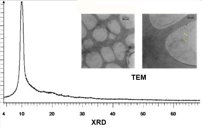
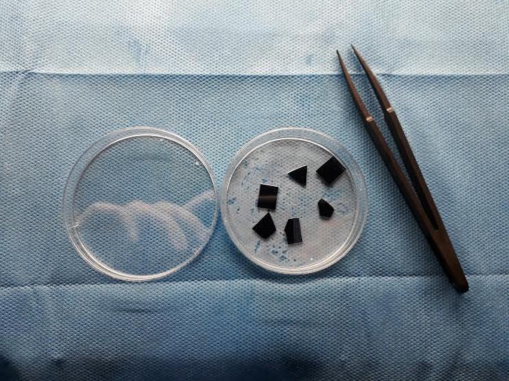
FESEM Image proves the sheet like structure of GO oxide and single peak on XRD diagram guarantees that there is some kind of lattice under test. The wafers were cut out of a 5-inch wafer by a scriber by hand and then rinsed with deionized water to ensure external particles and pollutants to be washed away. The colloidal solution was drop coated on 1×1 cm cut n-doped silicon wafers and was left in order to the solvents totally evaporated. The polished surface side of the wafers was chosen to drop solution on it. Following figure shows GO coated wafers ready for surface treatment.
An ordinary industrial engraving cutting machine was chosen to scan surface of the samples. Whole surface of the samples were scanned by CO2 laser to make sure all surface is exposed to laser beam. By rotating the samples by 90 degrees, the same task was done again. As the beam was scanning the samples at the air and without any inert atmosphere, the optics of machine was adjusted out of focus to prevent the surface from burning or any other chemical reaction in presence of oxygen.
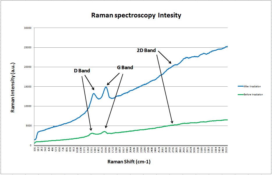
The Raman spectroscopy was performed to examine the functional groups. Raman spectrometer brand and model was TakRam N1-541 working with 532 nanometers wavelength. Following figure displays these results. Two vivid peaks can be seen around 1350 cm-1 and 1600 cm-1 which are named D-band and G-band in literature. Another peak known as 2D-band in literature is hardly can be observed around 2750 cm-1. In order to have a measuring factor to analyze the Raman intensities, intensity of D peak or D-band divided by intensity of G peak or G-band is generally utilized in research reports. For the GO film before irradiation this factor was calculated to be 0.881 and for the irradiated sample it was 0.893. Besides there is a right slight shift of D-band peak can be observed from the Raman test after reduction. The situation seems unchanged for G-band peak. These changes can prove the partially reduction of GO film on silicon wafer. In other words, functionalities which at general contain oxygen atoms are removed from the surface of the film.The low cost and prevention from using chemicals promises an easy to handle method of mass fabrication of graphene to make economical sensors in future.